integrating CMOS logic with silicon quantum dots
Scalable on-chip multiplexing of low-noise silicon electron and hole quantum dots
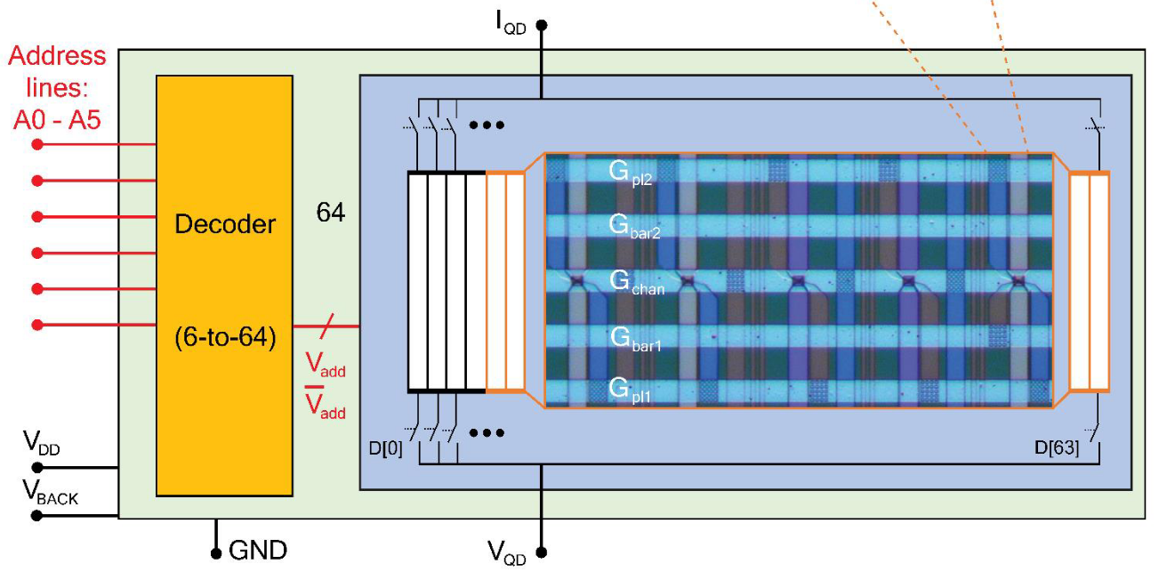
The scalability of the quantum processor technology is elemental in reaching fault-tolerant quantum computing. Owing to the maturity of silicon microelectronics, quantum bits (qubits) realized with spins in silicon quantum dots are considered among the most promising technologies for building scalable quantum computers. However, to realize quantum-dot-based high-fidelity quantum processing units several challenges need to be solved. In this respect, improving the charge noise environment of silicon quantum dot-based qubits and the development of ultra-low-power on-chip cryogenic classical complementary metal oxide semiconductor (CMOS) electronics for the manipulation and interfacing of the qubits are important milestones. We report scalable interfacing of highly tunable and ultra-low charge noise electron and hole quantum dots embedded in a 64-channel cryogenic CMOS multiplexer, which has less-than-detectable static power dissipation (< 1 pW) even at sub-1 K temperatures. Our integrated hybrid quantum-dot CMOS technology provides a route to scalable interfacing of up to millions of high-quality quantum dots enabling, for example, straightforward variability analysis and qubit geometry optimization, which are essential prerequisites for building fault-tolerant large-scale silicon-based quantum computers. At 5.6 K temperature, we find unprecedentedly low charge noise of 22 and 28 μeV/sqrt(Hz) at 1 Hz in the electrostatically defined few-electron and few-hole quantum dots, respectively. The low-noise quantum dots are realized by harnessing a custom CMOS process that utilizes a conventional doped-Poly-Si/SiO2/Si MOS stack. This approach provides lower charge noise background than high-k metal gate solutions and translates into higher spin qubit fidelities.